ProFIT Project HOTSTACK
A new wave of laser technology is on the rise, centered around high-energy pulsed solid-state lasers. These advanced systems can emit ultrashort optical pulses, ranging from megawatts to petawatts in energy, paving the way for generating diverse types of radiation.
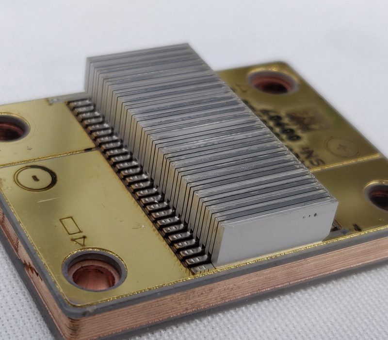
A critical component of these cutting-edge laser systems is the use of diode laser stacks. These stacks are pivotal in producing secondary beams, such as X-rays or particle beams, unlocking new possibilities in material processing, spectroscopy, and imaging previously unattainable with other technologies. This innovation allows companies to assess product quality without invasive methods, and researchers to expedite drug efficacy studies without the need for extensive facility wait times.

The HOTSTACK project is spearheading this technological leap by focusing on the development of significantly advanced diode laser and assembly technologies. Our aim is to introduce two types of high-power diode laser stacks as research prototypes. Our development efforts are concentrated on enhancing the repetition rate and energy of the optical pulses, while also streamlining the manufacturing process to reduce costs.
HOTSTACK is a “ProFIT Innovation” project and is co-financed from 2023 – 2025 with funds from the European Fund for Regional Development (ERDF) Berlin.
+++ Update: Because of a temporary project pause, the planned completion has been rescheduled for the end of 2026 +++
Project Partners
Trumpf GmbH is coordinating the HOTSTACK project and is also researching at its Berlin location on how to economically manufacture high-performance laser diodes. Within the HOTSTACK project, Trumpf is developing “Type 1” stacks with an industrial design, targeting the emerging secondary source industry. The goal is to create an exceptionally cost-effective and advanced industrial design. Trumpf aims to increase the average pump power per stack by approximately 20 times compared to existing systems, through higher pulse repetition rates and increased optical pulse power. This approach intends to achieve pulse powers exceeding 20 kW of laser power at room temperature for the first time, utilizing compact laser diode stacks with radiating areas of about 1 x 2 cm.
https://www.trumpf.com
In addition to developing “Type 1” configurations, “Type 2” stacks designed for research purposes will be developed. These will support investigations into cutting-edge laser systems with unprecedented energy levels, such as the upcoming EuPRAXIA project (EuPRAXIA facility). Goal is to enhance the average pump power by 100 times. Most of this research will be conducted at the Ferdinand-Braun-Institut.
High-energy laser systems require diode lasers in large quantities, but their production involves intricate manufacturing techniques, including epitaxial growth, structuring and etching of III-V wafers. It’s crucial to have reliable process control to fully grasp and manage these manufacturing steps. To this end, LayTec, in collaboration with FBH, will develop advanced integrated optical analysis methods. These methods will focus on both III-V epitaxial growth and wafer process technology, aiming to enhance process comprehension and management for such complex structures. The introduction of these innovative control techniques is expected to significantly boost the yield of diode laser production, thereby facilitating cost-efficient manufacturing of diode lasers. This development is crucial for supporting the extensive needs of high-energy laser systems.
https://www.laytec.de
Within the HOTSTACK project, Finetech is developing automation solutions aimed at ensuring a more cost-effective fabrication process (assembly, collimation) for the stacks. At the same time, the exploration of alternative bonding processes is pursued to increase performance, the safety of the production process, and to reduce manufacturing costs.
Research on innovative automation processes is being conducted in collaboration with Trumpf. Furthermore, the demonstration of innovative stack manufacturing processes with alternative bonding technologies such as sintering, thermo-compression, and reactive bonding is planned. These methods will be tested using heat sink materials and potentially more cost-effective stack configurations.
30+ Years of Laser Packaging Expertise by Finetech
Finetech offers a wide range of die bonders, including the automated FINEPLACER® femto product line. These products feature many innovative solutions for laser packaging, such as the Laser Activation Module for Reactive Multilayer Soldering (RMS), sophisticated tools for high-speed, high-precision, and high-quality laser diode soldering, and the Laser Substrate Heating for dense Chip-to-Wafer soldering/bonding, among others.
All providing an effective solution to the challenges encountered in 1st and 2nd level laser packaging.
Bringing the full packaging process into one system reduces dependencies on external vendors and tools, minimizes the need for purchasing and maintaining additional machines, optimizes assembly processes with single-system control and efficiency, and ensures precision bonding. This enhances thermal management and performance across all facets of laser bonding.
By using this element, you agree that your data will be transmitted to external services (https://www.youtube-nocookie.com) and that you have read our privacy policy.
Read our technical papers:


Embrace the power of our fully automated FINEPLACER® femto product line to revolutionize your laser production process, significantly reducing overheads and operational costs.
This strategic move not only enhances your production efficiency but also allows you to offer more competitive pricing to your customers by eliminating the extra costs tied to outsourcing.
The benefits are twofold: you’ll see an improved return on investment thanks to decreased production expenses, and your customers will appreciate high-quality products at more affordable prices.
- Significant Cost Reduction: Transition to in-house production with our femto line to avoid the markups of outsourcing, directly translating into cost savings for your business and lower prices for your customers.
- Enhanced Competitive Edge: With the ability to offer superior products at competitive prices, you’ll position your business as a leading player in the market, ready to capture more market share and drive growth.
- Reinvestment Opportunities: The savings you achieve can be reinvested into your business, whether it’s in research and development, expanding your product line, or exploring new markets, paving the way for sustained success and innovation.
Our FINEPLACER® femto product line enhances in-house laser assembly and second-level packaging, merging them into a single, fully automated process. By leveraging our proven CoS assembly technologies, you not only simplify your production line but also significantly reduce dependencies on external vendors and multiple processes in multiple machines.
This all-in-one solution simplifies logistics and enhances manufacturing control, ensuring reliability and efficiency in every step of your production.
- Single-System Efficiency: The FINEPLACER® femto product line integrates laser assembly and packaging, eliminating the need for multiple tools, processes and machinary.
- Automation Advantage: Fully automated systems enhance production speed and consistency, reducing manual intervention.
- Streamlined Manufacturing: Simplify your production line, achieving higher throughput and lower operational complexities.
Our expertise in tooling is unmatched, designed to deliver the utmost quality across all facets of laser bonding and packaging. Whether you’re grappling with co-planarity, wettability, smile and polarization, force, overhand or accommodating diode sizes large or small, our tools are engineered to ensure your success.
What are your benefits?
- Best eutectic soldering with precision alignment: Build perfect CoS and avoid catastrophic failure through perfect thermal conductivity by soldering management and perfect overhang alignment.
- Maintaining and controlling superior beam quality of laser diodes: Next generation laser tools for lowest possible stress while eutectic soldering for best repeatability in polarization and minimal wavelength shift.
- Precision in Every Aspect: From achieving perfect co-planarity and wettability to applying the right force, we make no compromises in ensuring your lasers are bonded with unmatched precision.
Our meticulous approach to the bonding process ensures that every aspect of the laser chip’s interaction with the substrate — from the bond line to surface contact and overhang — is optimized for maximum heat dissipation.
This precision in assembly not only enhances the reliability of your lasers in demanding operational environments but also significantly extends their lifespan while minimizing the need for maintenance.
- Precision Bonding for Enhanced Reliability: Our advanced bonding techniques ensure perfect alignment and contact, crucial for optimal thermal management and consistent performance under all conditions.
- Long-Term Cost Efficiency: The improved thermal handling capacity of our bonded laser systems leads to longer operational lifespans and lower maintenance requirements, translating into significant savings over time.
- Unwavering Performance in Demanding Environments: Trust our bonding solutions to maintain your laser’s efficiency and reliability, even in the most challenging operational scenarios, ensuring your applications run smoothly and without interruption.
Laser Activation Module
The innovative Laser Activation Module brings ultra-fast reactive soldering to our fully automated femto system, to not only accelerate the manufacturing process but also significantly elevate product quality.
This powerful synergy allows for the completion of both laser assembly and second-level packaging within a single, automated system.
By doing so, we drastically reduce subsequent process times, such as the usually time-intensive active alignment, or remove them completely such as the manual and bottleneck-prone steps of loading and running vacuum ovens for second-level assembly soldering.
- High-speed 2nd level packaging for multi-emitter: Time saving through reactive soldering comes with best relative placement accuracy between multiple laser sources reducing downstream process time such as active alignment.
- Versatility of our platform: Possibility to integrate LD manufacturing stages 1 and 2 into one single machine and for multiple laser module designs.
Laser Substrate Heating Module
The Laser Substrate Heater module enhances chip-to-substrate and chip-to-wafer assembly by delivering precise, localized heating for faster, more accurate processes. This method minimizes oxidation risks through rapid temperature cycles and does not require complex thermal expansion precautions.
Ideal for high-accuracy soldering, the technology uses an IR laser to efficiently heat components, reducing process time and eliminating the need for protective atmospheres during soldering. With its ability to process multiple substrates sequentially without transferring to a heating plate, Finetech’s solution offers streamlined production and superior assembly quality in electronic manufacturing.
Eutectic Bonding with Precision Tooling
Our eutectic bonding process with metal alloys like Au/Sn provide a number of advantages, e.g. high stability, high melting temperature, excellent resistance to corrosion, good wetting behavior, high thermal conductivity and high surface tension. If process gas is integrated into the process, the use of flux is not required, meaning that during bonding of e.g. optical components the risk of pollution is diminished.
As the melting point is rather high, eutectic bonding with Au/Sn is often combined with other soldering processes such as Indium bonding. When performing sequential bonding or step bonding processes, the use of different melting point materials will prevent previous joints from melting.
Our expertise in assembly tooling ensures unmatched quality in laser bonding and packaging, addressing challenges such as co-planarity, wettability, SMILE effect and force control with precision tools and guaranteeing optimal performance and reliability of your lasers.

Meet our FINEPLACER® femto Systems
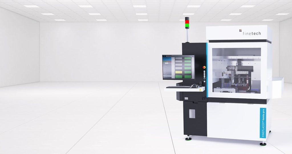
FINEPLACER® femto pro
The Efficient Solution for Advanced Packaging
High precision and versatility with a focus on reduced cost-per-bond and higher UPH.
The modular FINEPLACER® femto pro can be individually configured and upgraded in-field to support additional applications and technologies in the field of photonics.
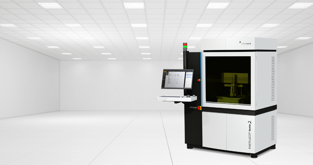
FINEPLACER® femto 2
Advanced Automated Sub-Micron Bonder
Fully-automated die bonder offers unrivaled flexibility for prototyping & production environments.
The modular design of the automated die bonder FINEPLACER® femto 2 can be individually configured and retrofitted at any time to support new applications and technologies.


