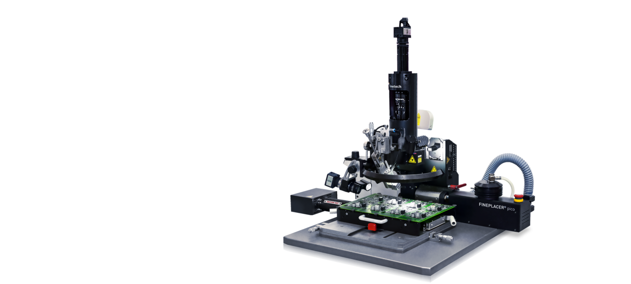
Hot Air SMD Rework Station
FINEPLACER® pico rs is an enhanced hot air rework station for assembly and rework of all types of SMD components.
The system is a bestseller for professional mobile device rework in high density environments. A high level of process modularity allows all rework process steps within one system. The FINEPLACER® pico rs system is at home in R&D, process development, prototyping and production environments.
Application area from 01005 up to large BGA on small to medium sized PCBs, with the goal to have highly reproducible soldering results.
"We have been partners with Finetech for over 15 years now and they have always been open to our needs. The support they provide is immeasurable – their engineering team is very accessible and everyone is well connected and deeply involved with each project. The quality we get is always at the highest level – from the first to the 2,000th board.”
Nafi Pajaziti
CEO, BMK Electronic Services
Key Facts*
- Full hot air rework system
- One system for rework and micro assembly
- Industry-leading thermal management
- Unique FINEPLACER® working principle
- Placement accuracy better 5 µm
- In-situ process observation in HD
- Data/media logging and reporting function
- Overlay vision alignment system (VAS) with fixed beam splitter
- 3-color LED illumination
- Full process access and easy programming
- Synchronized control of all process related parameters
- Software controlled top heater calibration
- Modular machine platform allows in-field retrofitting during entire service life
- Individual configurations with process modules
- Fully manual or semi-automatic machine versions
- Force controlled component handling
Applications & Processes
With a broad range of supported applications and technologies, our die bonding systems are ready to tackle any photonics application challenge in the industry. And as market requirements shift and new technologies emerge, their modular hardware and software architecture ensures maximum technological versatility over the entire service life.
Functions - Modules - Enhancements
Our die bonding solutions are as individual as our customers' requirements and offer a wide range of configuration options. In addition to the system's basic functions, which are part of the standard functional range, numerous process modules are available for each system, expanding the spectrum of photonic applications. Retrofittable at any time, they enable additional die bonding technologies and processes either directly or as part of a module package. A selection of functional enhancements and accessory systems make daily work with the die bonder easier and help to make certain technology and process sequences even more efficient.
Ensures safe handling of components from GelPak®, VR trays, waffle packs or tape holders.
Applying solder paste made easy by printing directly on the component | An “all in one“ solution for reworking QFN, SON and MLF components.
Integration of dispensing systems for applying flux, solder paste, adhesive or other pasty material. Various supported types like time-pressure or volume dispensers.
Local or full area bottom heater? A question of efficiency | Our approach ensures heat is provided only where it is needed to save energy and protect board and components.
Vision Alignment System with one camera and fixed beam splitter for an easy and direct alignment of the bonding partners.
Customized clamping solution for various shapes of PCBs.
For an economic use of nitrogen as hot gas, to save resources, energy and money.
Because reproducibility matters | Measures the temperature of a defined point on the board surface for reproducible process conditions.
Allows the in-situ observation of the working area during the soldering process.
Recycle BGA and CSP while saving time and money | Allows solder sphere arrays to be restored on custom specified BGA or CSP components after residual solder has been removed.
Allows precise residual solder removal in an inert atmosphere. Molten solder is easily removed from the board with powerful vacuum without disturbing any pads or solder resist.
Allow two opposite corners of a large component and its corresponding pad area on the substrate to be viewed under high magnification.
A small red point accelerates the working flow | Enables coarse position alignment of the table to the tool with the help of a laser spot.
Allows the heat transfer from the top with hot gas and chip specific tool design to control temperature from the chip direction.
Allows presentation of components from GelPak®, VR trays, waffle packs or tape holders as well as the support of dipping trays or cleaning units.
Allows the adaptation of the Vision Alignment System for an optimized view of components and substrates.
Technical Paper

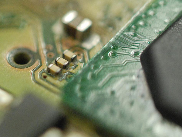
Rework of 01005 and 008004 Small Passives
008004 and 01005 small passive components are becoming more and more important these days (integration, miniaturization etc.). They allow particularly flat package designs when developing ultra-mobile electronic products such as functional modules,...
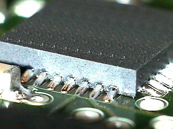